GR5526 (9)-Display Controller Driver Configuration Reference
[TOC]
1. Display controller
The Display Controller is a peripheral module unique to the GR5526 chip family. Refresh the result of GPU graphics rendering to the screen for display. The purpose of this article is to explain how to configure common drive timings.
1.1Initialization function parameter
The initialization function of the DC module is the graphics _ DC _ init, and the input parameter app _ graphics _ DC _ params _ t of the struct to be constructed is as follows:
| parameter | Explain | Value |
|---|---|---|
| mspi_mode | Data Mode | GDC_MODE_SPI |
| GDC_MODE_DSPI | ||
| GDC_MODE_QSPI | ||
| clock_freq | DC clock freq | GDC_CLOCK_FREQ_48MHz |
| GDC_CLOCK_FREQ_24MHz | ||
| GDC_CLOCK_FREQ_12MHz | ||
| GDC_CLOCK_FREQ_6MHz | ||
| GDC_CLOCK_FREQ_3MHz | ||
| clock_mode | DC clock mode | Generally, the GDC _ CLOCK _ MODE _ is 0. |
| tcsu_cycle | CS setup delay | Configure it as GDC _ TCSU _ CYCLE _ 1 without modification |
| layer_mode | Layer mode | It is enough to configure the GDC _ ONE _ LAYER _ MODE without modification |
| mipicfg_format | DC output format | GDC_MIPICFG_SPI_RGB565_OPT0 |
| GDC_MIPICFG_SPI_RGB888_OPT0 | ||
| GDC_MIPICFG_DSPI_RGB565_OPT0 | ||
| GDC_MIPICFG_DSPI_RGB888_OPT0 | ||
| GDC_MIPICFG_DSPI_RGB888_OPT1 | ||
| GDC_MIPICFG_QSPI_RGB565_OPT0 | ||
| GDC_MIPICFG_QSPI_RGB888_OPT0 | ||
| GDC_MIPICFG_SPI_RGB332_OPT0 | ||
| resolution_x | width resolution | |
| resolution_y | height resolution | |
| pins_cfg | Pin congigurations | The pins are controlled by hardware by default, and the relevant function pins can only be pinmux to the firmware pins. Driving parameter input mainly controls whether the corresponding pin is enabled |
The output timing diagram corresponding to each timing format of the mipicfg _ format is as follows:

Note: The time sequence in the above figure is determined by the member variable frame _ timing of the input parameter app _ graphics _ DC _ cmd _ t of the app _ graphics _ DC _ send _ single _ frame interface
Differences between GDC _ MIPICFG _ SPI _ RGB 565 _ OPT0 (SPI-4) and GDC _ MIPICFG _ DSPI _ RGB 565 _ OPT0:
The former DCX signal line, as the auxiliary of the D0 signal line, serves as the command data indication logic, and when the level is low, it indicates the control command transmitted by D0; When the level is high, it indicates the graphic data transmitted by D0
The latter DCX acts as D1, along with D0 for data representation, is 9 clks per pixel of data, with the highest CLK being used to indicate whether command (0) or data (1) is current
Function call reference:
    app_graphics_dc_params_t dc_params = {
        .mspi_mode  = GDC_MODE_QSPI,
        .clock_freq = GDC_CLOCK_FREQ_48MHz,
        .clock_mode = GDC_CLOCK_MODE_0,
        .tcsu_cycle = GDC_TCSU_CYCLE_1,
        .layer_mode = GDC_ONE_LAYER_MODE,
        .mipicfg_format = GDC_MIPICFG_QSPI_RGB565_OPT0,
        .resolution_x   = screen_w,
        .resolution_y   = screen_h,
        .pins_cfg = {
            .csn = {
                .pull = APP_IO_PULLUP,
                .enable = ENABLE,
            },
            .clk = {
                .pull = APP_IO_PULLUP,
                .enable = ENABLE,
            },
            .io0 = {
                .pull = APP_IO_PULLUP,
                .enable = ENABLE,
            },
            .io1 = {
                .pull = APP_IO_PULLUP,
                .enable = ENABLE,
            },
            .io2 = {
                .pull = APP_IO_PULLUP,
                .enable = ENABLE,
            },
            .io3 = {
                .pull = APP_IO_PULLUP,
                .enable = ENABLE,
            },
            .dcx = {
                .pull = APP_IO_PULLUP,
                .enable = DISABLE,
            },
        },
    };

    graphics_dc_init(&dc_params, NULL);
1.2 Frame data sending interface parameters
For the frame data sending function app _ graphics _ DC _ send _ single _ frame provided by DC, the input parameters are described as follows:
| 参数 | Explain |
|---|---|
| uint32_t which_layer | DC Layer, set to GRAPHICS _ DC _ LAYER _ 0, do not modify |
| app_graphics_dc_framelayer_t | See Figure 1 |
| app_graphics_dc_cmd_t | See Figure 2 |
| app_graphics_dc_access_type_e | The synchronous mode of the interface: -GDC _ ACCESS _ TYPE _ SYNC: synchronous call mode, the function returns after the screen is refreshed.-GDC _ ACCESS _ TYPE _ ASYNC: asynchronous call mode, the screen is refreshed and the result is returned through the callback function. |
Figure 1:
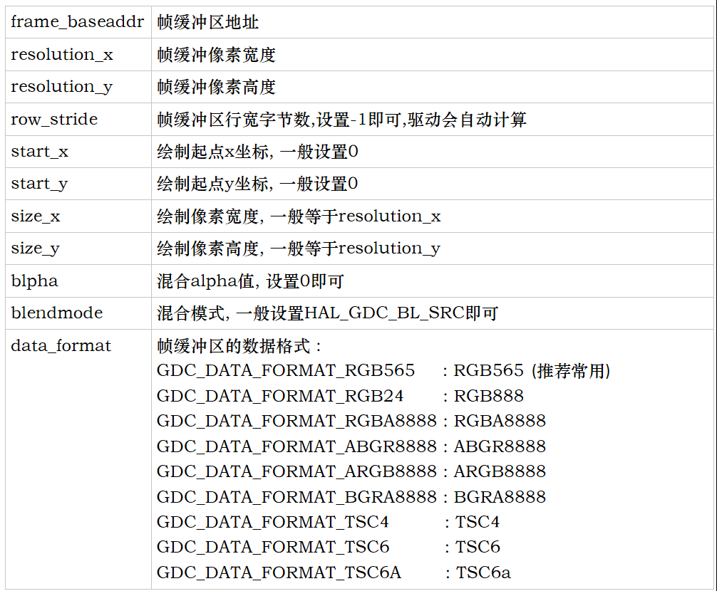
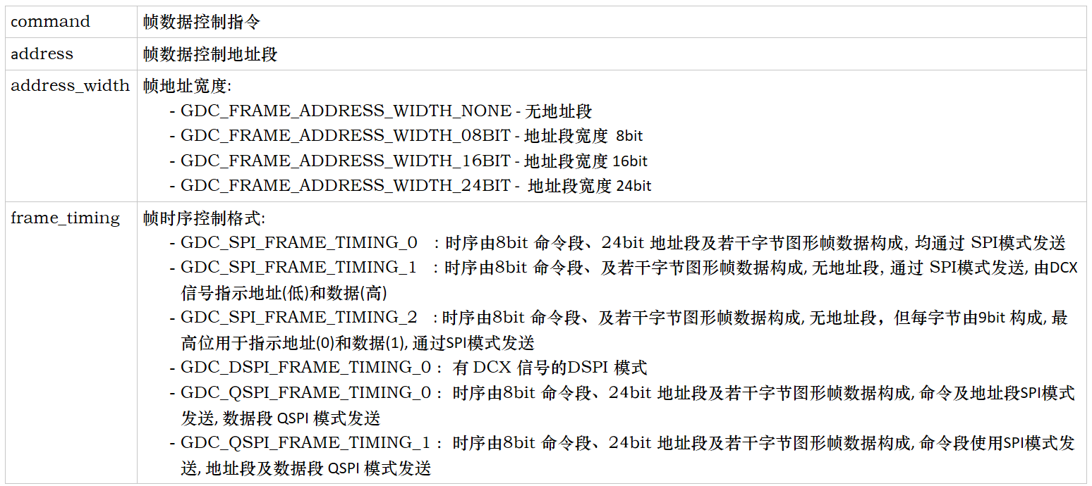
Figure 2:
Interface call reference (1):
Control command 0x38, control address segment 24 bit 0 x002c00, timing transmission mode: command is transmitted by SPI, address and data segment are transmitted by QSPI
The frame buffer format is GDC _ DATA _ FORMAT _ RGB 565, and the interface calling mode is asynchronous calling
app_graphics_dc_cmd_t dc_cmd = {
        .command = 0x38,
        .address = 0x002C00,
        .address_width = GDC_FRAME_ADDRESS_WIDTH_24BIT,
        .frame_timing  = GDC_QSPI_FRAME_TIMING_1,
    };

    app_graphics_dc_framelayer_t dc_layer = {
        .frame_baseaddr = buf,
        .resolution_x = w,
        .resolution_y = h,
        .row_stride = -1,
        .start_x = 0,
        .start_y = 0,
        .size_x = w,
        .size_y = h,
        .alpha = 0,
        .blendmode = HAL_GDC_BL_SRC,
        .data_format = (graphics_dc_data_format_e) GDC_DATA_FORMAT_RGB565,
    };

    app_graphics_dc_send_single_frame(GRAPHICS_DC_LAYER_0, &dc_layer, &dc_cmd, GDC_ACCESS_TYPE_ASYNC);
Interface call reference (2):
Control command 0x20, no address segment, time sequence sending format-GDC _ SPI _ FRAME _ TIMING _ 2
The buffer frame format is GDC _ DATA _ FORMAT _ RGB332, and the interface call mode is synchronous call
app_graphics_dc_cmd_t dc_cmd = {
        .command = 0x20,
        .address = 0x000000,
        .address_width = GDC_FRAME_ADDRESS_WIDTH_NONE,
        .frame_timing  = GDC_SPI_FRAME_TIMING_2,
    };

    app_graphics_dc_framelayer_t dc_layer = {
        .frame_baseaddr = buf,
        .resolution_x = w,
        .resolution_y = h,
        .row_stride = -1,
        .start_x = 0,
        .start_y = 0,
        .size_x = w,
        .size_y = h,
        .alpha = 0,
        .blendmode = HAL_GDC_BL_SRC,
        .data_format = (graphics_dc_data_format_e) GDC_DATA_FORMAT_RGB565,
    };

    app_graphics_dc_send_single_frame(GRAPHICS_DC_LAYER_0, &dc_layer, &dc_cmd, GDC_ACCESS_TYPE_SYNC);
2. Other DC Interface Timing Diagram
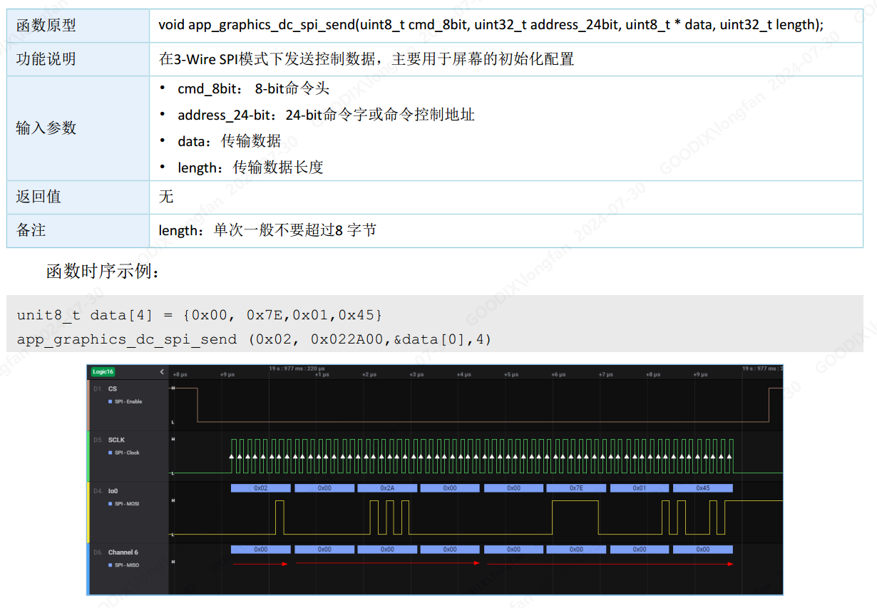
2.1 app_graphics_dc_spi_send
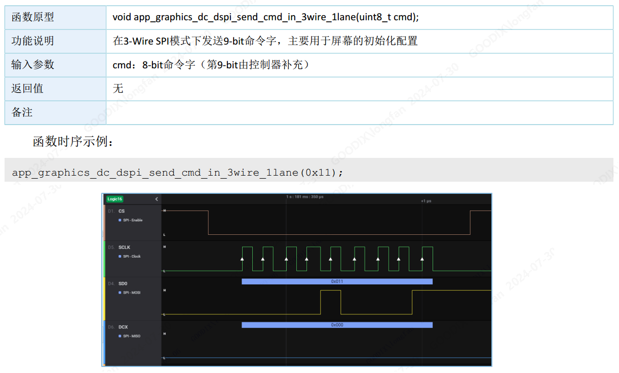
2.2 app_graphics_dc_dspi_send_cmd_in_3wire_1lane
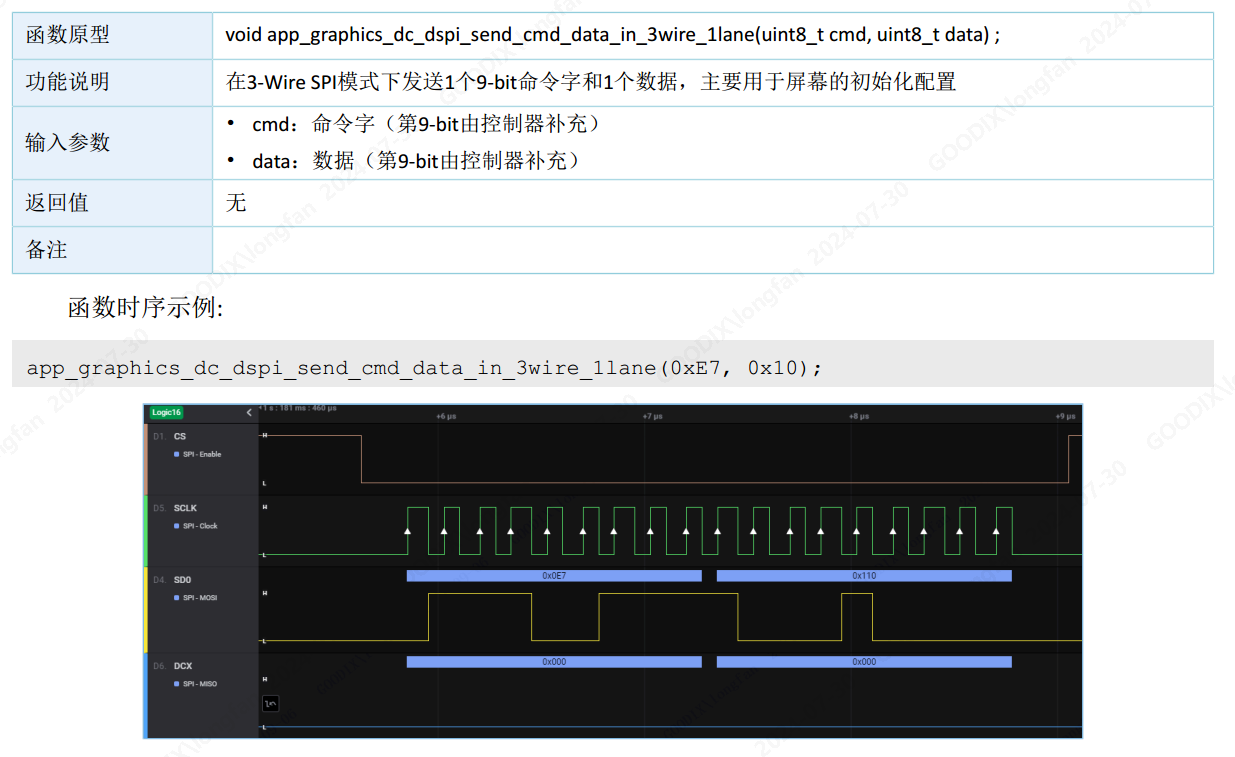
2.3 app_graphics_dc_dspi_send_cmd_data_in_3wire_1lane
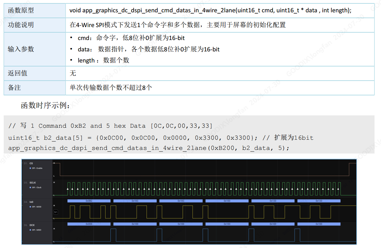
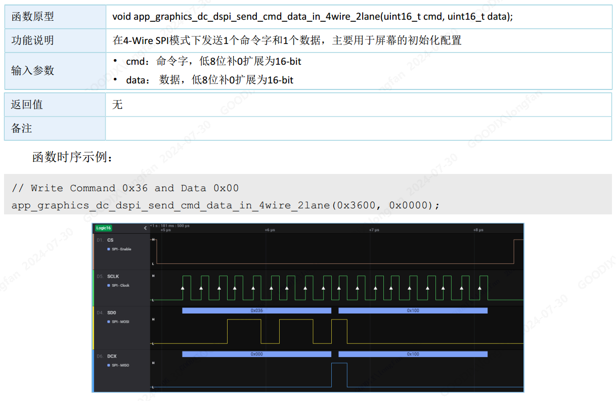
2.4 app_graphics_dc_dspi_send_cmd_data_in_4wire_2lane
2.5 app_graphics_dc_dspi_send_cmd_datas_in_4wire_2lane