FAQ for QSPI
1. What is the maximum frequency supported by QSPI?
The maximum frequency supported by the QSPI module is one-half of the maximum system frequency. The supported crossover coefficients are even numbers between 2 and 65535, and odd crossover frequencies are not supported.
The maximum frequency supported by each chip QSPI module is as follows:
The maximum main frequency of GR551x full series chips is 64 MHz, the maximum operating frequency of QSPI is 32 MHz, and the clock source is the system clock.
GR5525 full series chips have a maximum main frequency of 96 MHz, the maximum working frequency of QSPI is 48 MHz, and the clock source is the peripheral clock.
GR5526 full series chips have a maximum main frequency of 96 MHz, a maximum QSPI operating frequency of 48 MHz, and a peripheral clock source.
GR533x series chips have a maximum main frequency of 64 MHz, the maximum operating frequency of QSPI is 32 MHz, and the clock source is the peripheral clock.
2. QSPI Operation Mode Introduction
According to the data lines required for QSPI operation, QSPI can be configured to work in SPI, Dual SPI, and Quad SPI modes; of which the SPI mode is similar to the SPI Master module.
Under the QSPI module, the Dual SPI and Quad SPI modes are also known as Enhanced SPI mode. the GR5525 and GR5526 extend the capability of the Enhanced SPI mode to support Memory Map, which maps the NOR Flash and QSPI PSRAM memory devices mounted to the QSPI interface to the system’s bus address space, which can be accessed using Memory Map mode. The traditional API-based access to peripherals is called the register operating mode.
For a more detailed description of the operating modes, please refer to《GR5525刷屏指南》/《GR5526刷屏指南》
3. What is the reason for data end-sequence exception when using Memory Map mode to access external Flash?
For GR5525 and GR5526 chips, a flexible end-sequence mode has been added to the Memory Map mode, which allows the user to configure the readout end-sequence of the data according to his/her needs. This situation is caused by the mismatch between the desired data end-sequence and the configured end-sequence. Please refer to《GR5525刷屏指南》/《GR5526刷屏指南》for the description of data end sequence in QSPI Memory Map mode Configuration description. Use the driver interface app_qspi_mmap_set_endian_mode to configure the desired data end-order before accessing data.
4. Using traditional API interface (non-Memory Map mode) to read external Flash, the data does not match the desired data endian order.
Please refer to 《GR5525刷屏指南》/《GR5526刷屏指南》 on the description of read/write end-sequence, it should be that the data write and read out reverse order caused by using a mismatched transfer width. Please try to adjust the DMA data transfer width to modify the data end-order behavior. For example:
Using 8 bit transfer width mode results in 2 bytes of reverse order behavior, try adjusting the transfer width to 16 bit (or vice versa).
5. How to support QSPI module to use Memory Map mode to access Flash larger than 16 MB 4-byte address?
The app_qspi driver presets read commands for Flash with common 3-byte address (maximum addressing range 16 MB), if users need to extend the read commands with 4-byte address, please refer to the following definition. Take the EBH instruction of GD25Q256E chip as an example:
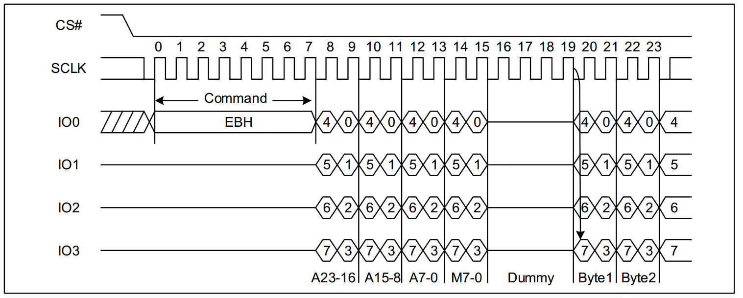
The timing format is:
Instruction EBH length 1 byte, sent via Single Wire mode.
The address is 4 bytes long and is sent in Quad mode.
The Mode bit occupies 2 clocks but does not need to be enabled and is grouped into the Dummy domain.
Dummy domain 4 clocks plus the 2 clocks occupied by the mode bit for a total of 6 clocks.
The rest is the Data domain.
The user extends the method of defining instructions:
Add custom enumeration value FLASH_MMAP_CMD_4READ_EBH_32 under _app_qspi.h_enumeration type app_qspi_flash_mmap_rd_cmd_e:
typedef enum {
    FLASH_MMAP_CMD_DREAD_3BH = 0x00, /**< 3BH in Dual */
    FLASH_MMAP_CMD_2READ_BBH = 0x01, /**< BBH in 2Read */
    FLASH_MMAP_CMD_2READ_BBH_SIOO = 0x02, /**< BBH in 2Read with SIOO mode */

    FLASH_MMAP_CMD_QREAD_6BH = 0x03, /**< 6BH in QRead */
    FLASH_MMAP_CMD_4READ_EBH = 0x04, /**< EBH in 4Read */
    FLASH_MMAP_CMD_4READ_EBH_SIOO = 0x05, /**< EBH in 4Read with SIOO mode */
    FLASH_MMAP_CMD_4READ_EBH_32 = 0x06, /**< ECH in 4Read with 32 bits address mode */
    FLASH_MMAP_CMD_READ_MAX, /**< ECH in 4Read with 32 bits address mode */ FLASH_MMAP_CMD_4READ_EBH_32 = 0x06, /**< ECH in 4Read with 32 bits address mode */
} app_qspi_flash_mmap_rd_cmd_e.
Add the instruction definition to the app_qspi.c file structure variable, taking care to add it at the same location as the index value of the enumeration value.
const qspi_memorymapped_t g_flash_typical_mmap_read_cmd[FLASH_MMAP_CMD_READ_MAX] =
{
    //...},
    [FLASH_MMAP_CMD_4READ_ECH_32] = {
        .x_endian_mode = QSPI_CONCURRENT_XIP_ENDIAN_MODE_0,
        .x_prefetch_en = QSPI_CONCURRENT_XIP_PREFETCH_DISABLE,
        .x_continous_xfer_en = QSPI_CONCURRENT_XIP_CONT_XFER_DISABLE,
        .x_instruction_en = QSPI_CONCURRENT_XIP_INST_ENABLE,
        .x_instruction_size = QSPI_CONCURRENT_XIP_INSTSIZE_8BIT,
        .x_address_size = QSPI_CONCURRENT_XIP_ADDRSIZE_32BIT,
        .x_inst_addr_transfer_format = QSPI_CONCURRENT_XIP_INST_IN_SPI_ADDR_IN_SPIFRF,
        .x_mode_bits_en = QSPI_CONCURRENT_XIP_MODE_BITS_DISABLE,
        .x_mode_bits_length = QSPI_CONCURRENT_XIP_MBL_8,
        .x_mode_bits_data = 0x00,
        .x_dummy_cycles = 6,
        .x_continous_xfer_toc = 0, .x_sioo_mode_bits_data = 0x00,
        .x_sioo_mode = QSPI_CONCURRENT_XIP_INST_SENT_EVERY_ACCESS,
        .x_data_frame_format = QSPI_CONCURRENT_XIP_FRF_QUAD_SPI,
        .x_instruction = 0xEB,
    }
}
When initializing the Memory Map mode of Flash, the read instruction references the instruction defined above to initialize it.
6. Accessing Flash using the QSPI sample project from the SDK fails, why?
Check whether the QSPI instance configuration of the sample project matches the actual hardware Flash connection.
The sample project provided by SDK is adapted to common Flash drivers. If the tested Flash is not the adapted Flash model, please check the Datasheet of Flash to see if it is compatible with the reference driver; if it is not compatible, please do the adapting by yourself.
If the hardware environment is harsh, such as flying wires and other scenarios, try to reduce the Flash communication frequency.
Check whether the clock mode configured by the driver matches the clock mode supported by Flash.
In addition, you can use a logic analyzer to capture the access Flash timing signals for analysis.
7. What are the reference programs for the QSPI peripheral?
The project ${SDK}/projects/peripheral/qspi/app_qspi provides an application reference for app_qspi driver to access NOR Flash, which can be run on the SK board accompanying the SDK. Users can use this sample project to understand the initial use of the QSPI APP interface.
In addition, for GR5525 and GR5526, the following QSPI peripheral driver reference is provided under the path ${SDK}/components/drivers_ext/qspi_device. Users can refer to it and develop it according to the specific situation of the product.
amo139_display_454.c/.h: Based on model FLS-AMO139WV334, resolution 454x54, driver IC SH8601A display development.
qspi_flash.c/.h: compatible with PUYA, XTX and other common NOR Flash driver reference.
qspi_nand_flash.c/.h: Driver reference based on NAND Flash DOSILICON.
qspi_psram.c/.h: PSRAM driver reference based on APMemory QSPI interface.
qspi_screen_390.c/.h: display driver reference based on Xinworld RM69330, adapted to 390p and 454p resolution.